The semiconductor industry is fast approaching the physical boundaries of silicon technology. As traditional transistor scaling yields diminishing returns, the pivot toward the third dimension has become an imperative. IBM has unveiled an ambitious roadmap for a 0.7nm process, a move poised to redefine the fundamental architecture of computing systems. This transition marks a decisive shift from planar scaling toward the comprehensive vertical synthesis of components.
Modern microelectronics has crossed the threshold into the era of sub-nanometer design. IBM has unveiled a 0.7nm (or 7-angstrom) process node, a milestone that effectively pushes fabrication to the atomic scale. At the heart of this breakthrough is the evolution of the Gate-All-Around (GAA) architecture, where the gate completely envelops the conducting channel, ensuring optimal current control and minimizing leakage.
The road to this point has been an arduous one. The GAA concept originated fifteen years ago through a collaboration between IBM and Samsung. Today, in partnership with Japan's Rapidus, the company is striving to bring 2nm chip production to scale. However, the transition from traditional FinFET transistors to GAA failed to address a fundamental limitation: on-chip element arrays remain essentially planar, constrained to a single two-dimensional plane.
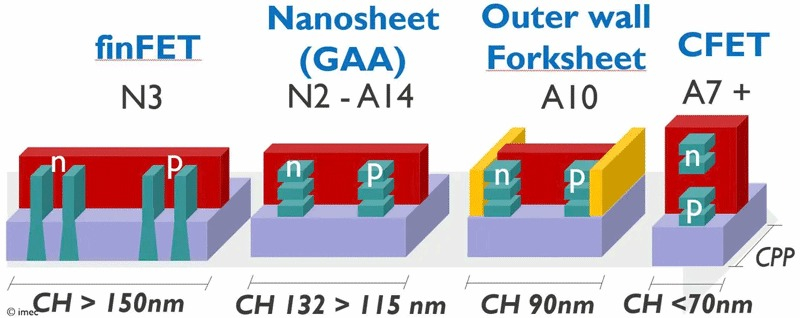
To shatter this ceiling, IBM is implementing the NanoStack concept. Rather than attempting to further compress transistors across the wafer's surface, engineers are proposing a vertical, offset stacking arrangement. This approach mirrors the Complementary FET (CFET) technology currently under development at the IMEC research center. Essentially, this represents a shift toward "true 3D" integration, where computing elements are layered atop one another, radically amplifying transistor density.
This architecture leverages ultra-thin dielectrics for layer isolation, enabling the independent design of upper and lower channels. The results are staggering: nearly 100 billion transistors can now be packed onto a die the size of a fingernail. This represents a twofold increase in density compared to the 2nm GAA technology introduced in 2021. To put this scale into perspective: the channel width in this new process is a mere 15 silicon atoms wide.
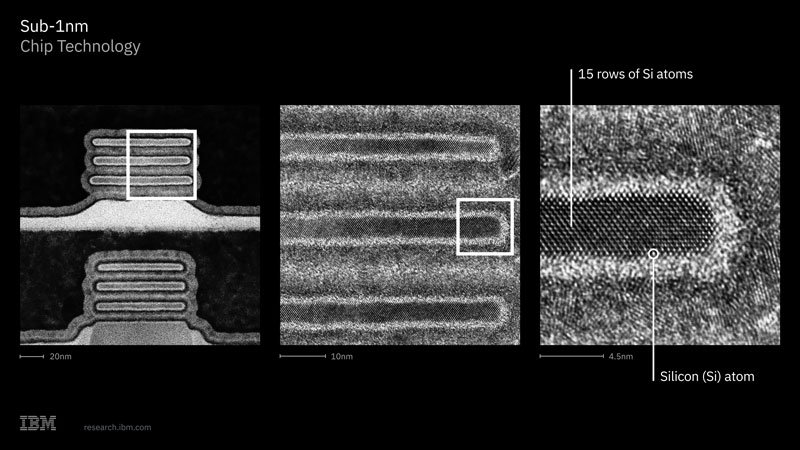
This technological leap translates directly into raw performance and energy efficiency. Projections suggest that the transition to 0.7nm could yield a performance boost of up to 50% or, alternatively, a 70% increase in energy efficiency over the 2nm process.
Of particular significance is the 40% improvement in SRAM scaling. In the era of AI dominance, this becomes a critical factor. The "memory wall"—the phenomenon where moving data between the processor and external memory consumes massive amounts of energy and generates excessive heat—remains a primary bottleneck. The more high-speed memory that can be integrated directly into the compute block, the more efficiently AI accelerators operate, simplifying the cooling challenges of massive data centers.
Commercial realization of this process is slated for 2031. By then, the semiconductor industry must fully transition from two-dimensional thinking to comprehensive vertical synthesis, ensuring the continued evolution of Moore's Law even in the face of the rigid physical constraints of matter.

 The Evolution of the Apple Home Ecosystem