The global semiconductor race is currently defined by a relentless pursuit of cutting-edge nanometer nodes and the critical challenge of stabilizing wafer yields. For years, Intel has fought to reclaim its technological primacy, battling systemic hurdles within its manufacturing cycles. Recent data suggest the company has reached a pivotal tipping point in the development of its 18A node. The transition from experimental prototypes to sustainable high-volume manufacturing represents a strategic victory in Intel's broader ambition to establish a viable, full-scale foundry business.
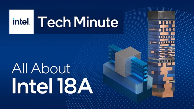
The road to semiconductor perfection is invariably paved with the struggle for viable yields. For Intel, the 18A process node represents far more than a mere milestone on its roadmap; it is a high-stakes survival test in a brutal competition with TSMC and Samsung. According to the latest data from BlueFin Research Partners, the company has finally navigated the volatility of early production, achieving a stable output of functional dies—a critical threshold that renders the process both economically viable and scalable.
The primary indicator of this success is the pace of optimization: for several months, yield rates have demonstrated a steady climb of approximately 7% per month. In the semiconductor industry, such momentum signals that the process's "teething issues" have been resolved and production lines are calibrated with surgical precision. From a technical standpoint, this translates to a low defect density (D0), which has reportedly dropped to the 0.1–0.2 range. For a mature process, these figures represent the gold standard, ensuring minimal waste during mass production.
Currently, the manufacturing foundation of 18A rests on two primary sites: Fab 52 in Phoenix, Arizona, and facilities in Hillsboro, Oregon. Combined output has reached 30,000 wafers per month. While this volume is sufficient to meet internal demands—specifically for the Panther Lake processor family—further capacity expansion will be essential to execute Intel's broader strategy and support additional internal product lines.
Intel’s strategy, however, extends beyond a single node. Preparations are already underway for the deployment of the modified 18A-P process. Pilot production has launched at the D1X site in Oregon, with Fab 62 slated to become the primary hub for its long-term scaling. Even more ambitious is the transition to the 14A node. Initial pilot runs appear promising; the company intends to use the D1X plant for primary deployment before shifting the bulk of production to new facilities in Ohio.
For the external market, under the Intel Foundry umbrella, the strategic focus will center on 18A-P, 18A-PT, and the upcoming 14A. The latter is expected to be available for pilot production in 2028, with a full commercial launch scheduled for 2029. Ultimately, the stabilization of 18A provides the necessary foundation of trust for third-party clients, transforming Intel from a proprietary chipmaker into a formidable technological partner capable of competing in the global contract semiconductor market.
 The Price of Acceleration: CXMT’s Rapid Push into Memory