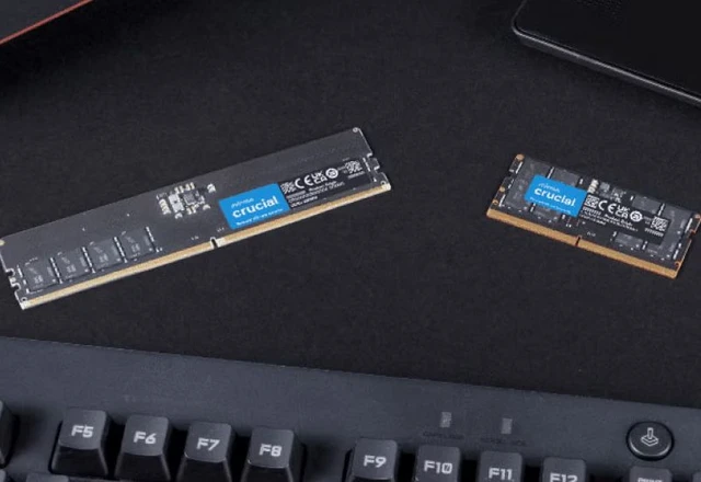
The global AI surge has triggered an unprecedented shortage of high-performance memory, elevating semiconductors to the status of a strategic resource for the digital age. In response, South Korea’s tech titans are deploying a sweeping strategy designed to fortify their industrial sovereignty. The multi-billion dollar investments poured into Samsung and SK hynix are intended to do more than merely expand manufacturing capacity; they are a calculated move to cement the region's dominance within the global supply chain. This shift signals the dawn of a new phase in the hardware arms race—one where the competitive edge lies in the synergy between raw production power and cutting-edge chip packaging techniques.
The contemporary IT landscape is defined by uncompromising demands for data storage and processing. The deployment of massive language models and neural networks requires not only raw GPU computing power but also colossal volumes of ultra-fast memory. In this context, SK hynix’s strategy reads like a surgical strike aimed at the market's most critical vulnerabilities. The company plans to invest 100 trillion won (approximately $64 billion) to expand its capacity, operating on the conviction that demand for NAND flash memory will continue to outpace supply.
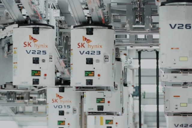
This strategic offensive is divided into two primary fronts. By 2029, the company will allocate 80 trillion won toward the construction of a new NAND production facility, establishing a vital buffer against potential shortages. Simultaneously, by the end of 2027, a specialized chip packaging plant with a budget of 20 trillion won will be deployed in Cheongju. Central to this effort is the M17 plant, with construction slated to begin next year. It is crucial to recognize that modern "packaging" is no longer merely a final assembly step; it is a sophisticated technological process that enables the integration of multiple dies into a single module. This is the cornerstone of High Bandwidth Memory (HBM), without which the operation of modern AI accelerators would be impossible.
Samsung, for its part, is implementing a more comprehensive, ecosystem-driven approach. The company's 140 trillion won ($90 billion) investment plan extends beyond semiconductors to encompass adjacent high-tech industries in the Chungcheong province. This move effectively transforms the region into a full-scale technological hub, where chip fabrication is seamlessly integrated with the development of advanced materials and components.
A significant portion of these funds—67 trillion won—will be directed toward the development of Samsung Display in Asan and Cheonan. An additional 56 trillion won will be invested by Samsung Electronics into the creation of high-speed memory packaging plants in Onyang and Cheonan, placing the company in head-to-head competition with SK hynix for dominance in the advanced data interface segment.
However, Samsung’s strategic horizon extends much further. By 2040, the company intends to complete a cycle of deep modernization: Samsung SDI will invest 9 trillion won into the R&D and production of next-generation batteries, while Samsung Electro-Mechanics will allocate 8 trillion won to develop cutting-edge materials for server-grade chip packaging and cultivate human capital in Sejong.
The sheer scale of these capital expenditures signals a fundamental shift: the battle for AI supremacy has moved from the software layer to the realm of materials science and industrial scaling. Establishing a closed-loop cycle—stretching from material science and wafer fabrication to complex packaging and server-level integration—is becoming the only viable way to maintain a competitive edge for decades to come.
 The Evolution of the Apple Home Ecosystem