The semiconductor industry is witnessing a fundamental paradigm shift, as image sensors evolve from simple light-capture tools into sophisticated sensory organs for artificial intelligence. In the global race for dominance in computer vision and autonomous systems, maintaining technological parity has become an existential imperative. The alliance between Sony and TSMC, cemented by multi-billion dollar investments, is designed to establish a new hardware standard for the era of "physical AI." This partnership fuses unique expertise in sensor development with the unparalleled precision of world-class foundry manufacturing.
The strategic alliance between tech titans Sony and TSMC is entering a new phase of scaling. The foundation of this partnership was the establishment of JSAM, a joint venture in Kumamoto already tasked with the contract manufacturing of image sensors. However, current capacities have proven insufficient for the Japanese corporation's ambitions, leading to the decision to construct a specialized plant with total investments reaching $6.3 billion.
The structure of the new enterprise grants Sony a majority stake of 60%, with TSMC holding the remaining 40%. The financial magnitude of the project is staggering: for Sony’s semiconductor division, such capital expenditures are comparable to a four-year development budget. For context, this figure approaches the $8.6 billion TSMC previously invested in its first contract plant within the same region. It is expected that a significant portion of these costs will be covered by government subsidies, underscoring the project's strategic importance to Japan's national economy.
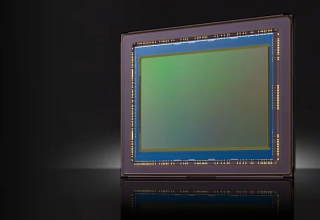
The formal establishment of the joint venture is slated for completion by the end of March next year, with full-scale production expected by 2029. This move represents more than a mere increase in output; it is a qualitative leap in technology. The new sensors will be engineered for deep integration with artificial intelligence systems, enabling devices to recognize objects with unprecedented precision and speed. The primary beneficiaries will extend beyond giants like Apple to entire industries—from robotics to autonomous driving systems, where the image sensor serves as a critical safety node.
The geographical choice fell on the city of Koshi in Kumamoto Prefecture. This decision was driven not only by the presence of Sony's specialized plants and future R&D centers but also by the rigorous infrastructural demands of semiconductor manufacturing. The region offers ample water resources and stable access to renewable energy. By leveraging solar panels and geothermal sources, the facility aims to minimize power supply risks that could arise from a reliance on traditional grids during unstable weather conditions.
In a global context, this move is a calculated response to mounting competitive pressure. Although Sony controls approximately half of the global image sensor market, its position is being seriously challenged by Samsung Electronics and OmniVision. The synergy with TSMC allows Sony to delegate the most complex lithography and fabrication processes to the world's leading contract manufacturer while maintaining its leadership in sensor architecture and design. For TSMC, this union provides access to unique expertise in creating components that will form the bedrock of "physical AI"—a frontier where digital intelligence gains the ability to interact fully with the material world.
 The Price of Acceleration: CXMT’s Rapid Push into Memory