The global semiconductor industry is entering a phase of extreme technological compression, where the battle for supremacy is fought at the scale of single-digit nanometers. Samsung Electronics is responding to this challenge through a massive expansion of its manufacturing footprint, shifting the strategic center of gravity for its foundry operations to the United States. This pivot toward 2nm and 1.4nm process nodes is a direct response to the explosive growth in demand fueled by the artificial intelligence sector. In this high-stakes race, the company aims not only to close the gap with the market leader but to fundamentally overhaul its entire economic model.
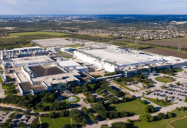
The global microelectronics landscape is currently undergoing a profound structural shift: the era of mobile chip dominance is giving way to the age of High-Performance Computing (HPC) and generative AI. In response, Samsung Electronics is entering an aggressive phase of capacity expansion. The epicenter of this strategy is Texas, where the company plans to launch its first advanced contract manufacturing facility in Taylor and is already laying the groundwork for a second adjacent plant.
The primary catalyst for this expansion is the surging demand for 2nm and 1.4nm process nodes. Currently, capacity ramp-up lags behind market requirements, creating a palpable supply deficit. Samsung aims to bridge this gap by scaling its footprint in Texas and other key regions—albeit pragmatically, ensuring that expansion remains phased and strictly aligned with actual demand to mitigate the risks of over-investment.
Long-term strategic planning is central to this pivot. By 2026, the company anticipates a doubling of order volumes for its 2nm chips compared to the previous year. This trend underscores growing client confidence in Samsung’s technological stack, particularly its aggressive development of Gate-All-Around (GAA) architecture, designed to optimize leakage current and enhance transistor power efficiency.
The economic dividends of this strategy are already manifesting. Achieving full utilization across production lines for sub-8nm processes allows the company to significantly drive down the unit cost per die through economies of scale. This provides a critical foundation for the foundry division to pivot away from losses and realize a marked improvement in profitability during the second half of the year.
Despite this upward trajectory, Samsung remains in the shadow of TSMC. While the Taiwanese giant derives over 75% of its revenue from advanced process nodes, the South Korean manufacturer's share is currently approaching the 50% mark. Nevertheless, the strategic direction is sound: reliance on the volatile mobile device market is waning. The contribution of AI and HPC to Samsung Foundry’s revenue has climbed from 20% to over 30% within a year, confirming a successful diversification strategy and a transition toward a more resilient, technologically independent ecosystem.
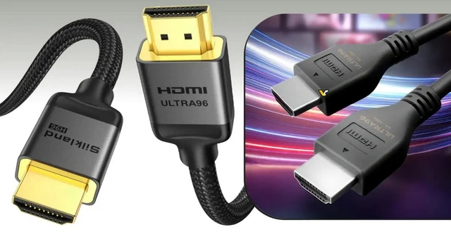 HDMI 2.2: The New Standard for Data Transmission