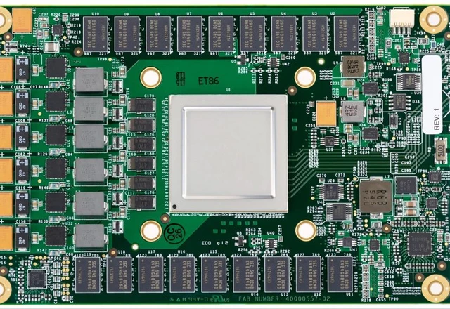
The global AI arms race has fundamentally shifted; the battleground is no longer defined by algorithmic elegance, but by the physical constraints of silicon. Today, the efficacy of neural networks is dictated less by the purity of the code and more by the hardware's capacity to move massive datasets with near-zero latency. Setting the pace for the entire industry, Nvidia is aggressively accelerating the rollout of its next-generation "Feynman" accelerators. This transition demands an unprecedented scaling of production capacity from TSMC, alongside the implementation of radically new chip packaging architectures.
The latter half of 2028 is poised to be a watershed moment for the high-performance computing (HPC) industry with the market debut of the Feynman accelerators. According to sources in Taiwan, Nvidia is significantly accelerating its preparation timeline, imposing rigorous demands on its suppliers. This shift represents more than just a transition to TSMC's A16 process; it is a fundamental transformation in the very philosophy of semiconductor assembly.
The strategic pivot centers on the adoption of advanced packaging methodologies. At the forefront are System on Integrated Chips (SoIC) 3D packaging and Co-Packaged Optics (CPO). While traditional chip-to-chip data transfer methods are beginning to hit a "glass ceiling" regarding power consumption and throughput, CPO allows optical interfaces to be integrated directly into the processor's package. This paves the way for bandwidth reaching 400 TB/s—a critical requirement for training next-generation models where data volumes are growing exponentially.
For TSMC, Nvidia's ambitions necessitate an urgent overhaul of its production infrastructure. Specifically, the company is forced to expedite the construction of the AP7 and AP8 fabs, dedicated to SoIC processing. Initial projections of 20,000 silicon wafers per month by the end of 2026 have been deemed insufficient. The target has now shifted: capacity must scale to 50,000 wafers monthly by the end of 2027. This has led to the accelerated deployment of engineering networks and the installation of cleanroom equipment ahead of schedule.
The Feynman accelerators represent a sophisticated technological stack, fusing the A16 process, SoIC 3D integration, customized HBM memory, and the aforementioned optical interconnects. Notably, this expansion benefits TSMC beyond its partnership with Nvidia, as SoIC technology will be highly sought after by other clients striving for maximum transistor and memory density.
Parallel to these developments, TSMC continues its progress on 2-nanometer solutions. In this segment, the outlook remains stable: the production of Apple's A20 Pro processors is proceeding according to plan, with yield rates remaining within acceptable limits. However, a different systemic issue has emerged—a DRAM shortage. Due to a lack of components, TSMC has accumulated a stockpile of A20 Pro processors valued at approximately $1 billion, which are effectively idling while awaiting memory chip integration. In this instance, a specialized packaging solution tailored for Apple is being utilized—one that experts describe as the mobile equivalent of CoWoS technology.
Simultaneously, there is a steady trend toward the development of proprietary AI silicon by cloud hyperscalers. For instance, TSMC plans to ship over 300,000 units of Microsoft's Maia 300 by the end of next year. This confirms a broader market shift toward bespoke hardware optimized for specific neural network tasks. Starting in mid-year, TSMC will begin expanding its CPO packaging capacity, providing the foundation for the ultra-high-speed interconnects essential for operating massive computing clusters.
 The Price of Acceleration: CXMT’s Rapid Push into Memory