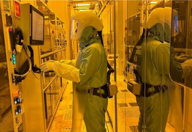
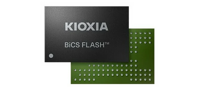
The semiconductor industry is currently undergoing a period of profound transformation, catalyzed by the meteoric rise of generative AI. As the demand for ultra-fast data access becomes a critical driver for the evolution of mobile devices and personal computers, Kioxia has unveiled its latest innovation: the ninth generation of BiCS FLASH memory. The company's technological stack is engineered to strike an optimal balance between storage density and interface throughput.
The evolution of non-volatile memory is currently defined by vertical scaling, where layer count has become the primary benchmark of technological superiority. Kioxia is now entering the test sampling phase for its 1 Tbit Triple-Level Cell (TLC) NAND, engineered using the ninth generation of BiCS FLASH 3D technology. These 230-layer chips are more than just an iterative update; they represent a strategic response to the demands of AI-driven hardware, where data exchange between storage and processor frequently becomes the critical bottleneck.
The technological core of these new chips rests on two fundamental innovations: CMOS Direct Bonded to Array (CBA) and On-Pitch Select Gate Drain (OPS). The CBA method enables the direct bonding of the control logic circuitry to the memory array, radically reducing die area and lowering power consumption. Simultaneously, OPS technology optimizes select gate geometry, allowing for increased cell density without compromising electrical stability. This approach allows Kioxia to scale layer counts effectively while maintaining high reliability for data read/write operations.
A key highlight is the NAND interface throughput, which has reached 4.8 Gbps in the ninth generation—a 33% increase over its predecessor. Effectively, Kioxia has pushed the performance of its "standard" high-performance segment to match that of tenth-generation flagship solutions, while maintaining a more sustainable production cost.
The company's strategy involves the development of two parallel product lines. The ninth generation targets the mass high-performance market, offering an optimal balance of cost and speed. In contrast, the tenth generation focuses on extreme density and peak performance for the most demanding enterprise workloads.
The primary beneficiaries of this 230-layer memory will be manufacturers of laptops, PCs, and modern smartphones equipped with integrated NPUs (Neural Processing Units). In devices with small to medium-capacity drives, high interface speeds are critical for running local Large Language Models (LLMs) and other AI tools that require the instantaneous loading of model weights from storage into active memory. Consequently, Kioxia is laying the groundwork for a new generation of "intelligent" hardware, where data access speed becomes as pivotal a metric as raw storage capacity.
 Anthropic’s Strategic Financial Surge Ahead of Its IPO