The semiconductor industry is currently locked in a relentless battle for every single angstrom. Intel, having spent years wrestling with its own erratic roadmaps, is now orchestrating a sweeping technological comeback. The new 14A process is more than just another milestone in miniaturization; it is a critical litmus test of the company's ability to maintain stable wafer yields. Recent data suggests that Intel may have finally broken the vicious cycle of manufacturing failures that has plagued the company for the last decade.
Only a year ago, Intel's executive leadership expressed palpable skepticism regarding the viability and timeline of the 14A angstrom process. Yet, in a remarkably short window, the company's rhetoric has shifted radically. Today, Intel claims an unprecedented trajectory in defect density reduction, asserting that 14A's performance metrics surpass those of every technological node the company has implemented since the transition to the 22-nanometer standard.
To grasp the magnitude of this claim, one must look to history. The 22nm node represented a pivotal, albeit agonizing, era for Intel; it marked the introduction of FinFET (fin field-effect transistor) architecture, which allowed the company to bypass the limitations of traditional planar structures. However, this triumph was overshadowed by a subsequent systemic crisis. The failure to transition to the 10nm process effectively forced Intel to "freeze" its 14nm technology, optimizing it indefinitely to meet market demand amidst a production collapse.
The complexity of mastering new fabrication nodes is best illustrated by the concept of "stepping"—the iterative process of correcting errors in chip topology. While processors based on the Nehalem and Lynnfield architectures reached the market with early revisions (C0 and B1, respectively), the 22nm-based Ivy Bridge required refinement up to stepping E1 before yields became acceptable for mass shipment. This pattern underscores a fundamental law of microelectronics: as the process node shrinks, risks escalate, and achieving high yields becomes exponentially more difficult. This is precisely why 14A was initially perceived as a project with an extreme risk profile.
Intel's current trajectory appears promising. This October, the developer toolkit for those utilizing Intel Foundry services will transition to version 0.9. This is a critical milestone, signaling that the software is ready for the creation of the first physical chip samples. Pilot production is slated to begin next year, with full-scale mass production scheduled for 2028.
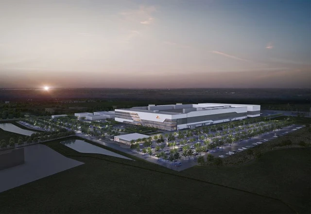
To realize these ambitions, the company is deploying a massive infrastructural network. A central role will be played by the new Fab 62 in Arizona. Simultaneously, an experimental line in Oregon—currently operating the Intel 18A-P process—will be retooled. Following this modernization, the site will become a serial production hub for 14A. Additional capacity will be deployed at a new complex in Ohio, the construction of which had previously been temporarily frozen.
The technological stack is also being bolstered at the post-processing stage. By the end of 2027, Intel's clients will gain access to the advanced EMIB-T packaging system. This 2.5D interconnect technology enables the integration of multiple chiplets into a single module with minimal latency—a critical requirement for modern AI accelerators and high-performance computing (HPC). In doing so, Intel aims to create a closed-loop ecosystem: from the ultra-precise 14A lithography process to sophisticated final assembly, reclaiming its status as the industry's technological vanguard.

 Nvidia’s Technological Pragmatism in the Open-Model Race