The modern AI arms race has hit a critical impasse known as the "memory wall," where the bandwidth of the storage subsystem has become the primary bottleneck stifling performance. While traditional HBM-based solutions are highly efficient, they are becoming prohibitively expensive and complex to manufacture due to their rigid dependence on silicon interposers. In response to this challenge, Intel has introduced Cross-Batch Memory (XBM), a concept that proposes a radical reimagining of memory's physical architecture. This technology seeks to decouple accelerators from these manufacturing constraints and push data density to an entirely new frontier.
The fundamental bottleneck facing modern AI accelerators is the widening gap between computational throughput and the speed of data transfer between the processor and memory. Currently, the industry relies on the High Bandwidth Memory (HBM) standard, where DRAM dies are vertically stacked and connected to a logic layer via through-silicon vias (TSVs). However, linking this stack to a GPU or CPU requires a silicon interposer—a complex intermediate substrate featuring a massive array of precision traces. This architecture makes production prohibitively expensive and leaves the entire market dependent on the limited capacity of advanced packaging lines, such as TSMC’s CoWoS.
Intel XBM seeks to disrupt this paradigm by replacing costly interposers with a native chiplet interface, UCIe. In this conceptual framework, the DRAM block connects to an I/O interface operating at 32 GT/s, allowing the module to maintain a footprint comparable to the upcoming HBM4 standard while significantly streamlining the assembly process.
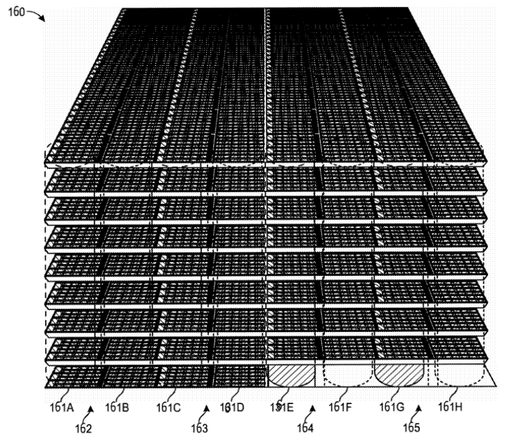
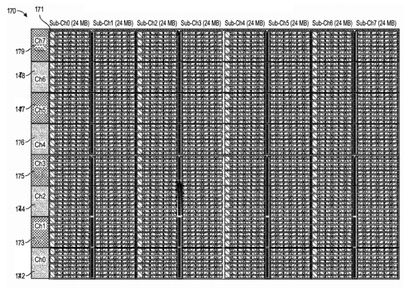
The technical implementation of XBM is built upon a rigorous hierarchy. Each memory die contains 768 data blocks organized in a 32x24 grid. These blocks are grouped into eight primary channels, each further subdivided into eight sub-channels. Depending on the configuration, these dies can be stacked in 8 or 16 layers, allowing the capacity of a single module to scale from 0.5 to 5.0 GB. The entire data flow is managed via a base die, with the channels operating at a frequency of 2 GHz.
However, the most audacious engineering feat in XBM is the migration of memory cells into the metallization layers. In conventional DRAM, cells are created during the FEOL (Front-End-of-Line) stage—directly within the base silicon layer alongside the transistors. Intel proposes utilizing the BEOL (Back-End-of-Line) stage, placing 1T1C (one transistor, one capacitor) cells within the upper interconnect layers using thin-film transistors. This approach "offloads" the silicon substrate and dramatically increases element density, bypassing the physical constraints of traditional layouts.

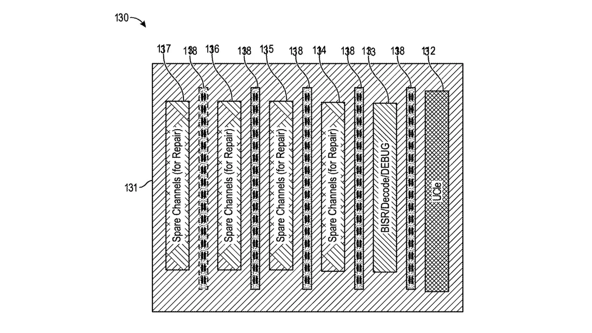
The shift toward complex 3D structures inevitably introduces yield challenges. To mitigate these risks, XBM integrates a sophisticated self-diagnostic and fault-tolerance system. The base die is equipped with a Built-In Self-Repair (BISR) mechanism and dedicated redundant channels. Combined with a Known Good Die (KGD) pre-testing strategy, the system can replace defective or thermally degraded cells with redundant arrays in real time. For servers operating 24/7 under extreme AI workloads, such redundancy becomes a critical factor for reliability.
Parallel to the electrical circuitry, Intel is optimizing the module's physical geometry. In traditional Memory-on-Package (MoP) approaches, an intermediate substrate is used, which adds an unnecessary 300–350 microns of thickness and impairs heat dissipation. The XBM patent proposes either placing the memory die directly on the package substrate or utilizing a "reversed overhang" architecture. This significantly reduces the overall module height, improves the thermal profile, and protects the chip from mechanical deformation.
It is crucial to understand that XBM is not Intel's only gambit. The company is simultaneously developing ZAM (Z-Angle Memory) in collaboration with SAIMEMORY, which focuses on the direct bonding of standard DRAM dies. While ZAM is an attempt to optimize existing components, XBM represents a fundamental reimagining of the memory transistor itself and its integration into the system.
Despite the elegance of the concept, XBM remains in the patent application stage. Implementing memory within metallization layers has yet to be proven in mass production, and the UCIe interface has its own inherent speed limits. Nevertheless, if Intel succeeds in bringing these ideas to silicon, the industry will gain a powerful tool to bypass the packaging capacity crisis, effectively transforming a complex materials science problem into a task of geometric optimization.
 iPhone 17: Dominating the Global Market