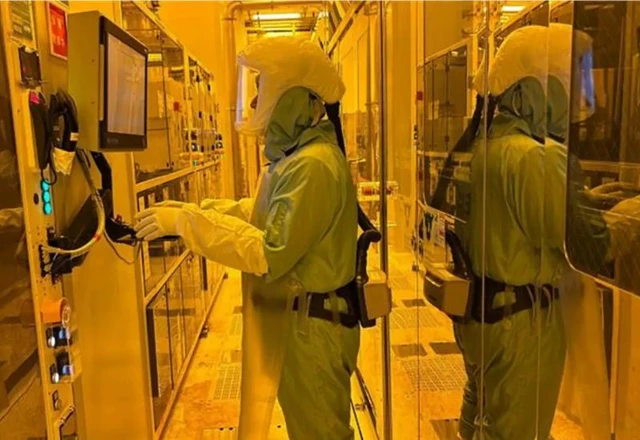
The global AI arms race is shifting its center of gravity from algorithmic optimization to the tangible reality of semiconductor manufacturing. Google, which has long cultivated its proprietary Tensor Processing Units (TPUs), is now gearing up for an unprecedented scale-up of its production capabilities. The company's roadmap for the coming years envisions scaling output to levels that rival those of the current market hegemon, Nvidia. This strategic pivot is designed to secure technological sovereignty and guarantee total independence for the tech giant's cloud infrastructure.
The AI industry is entering a phase where raw per-chip performance is no longer the sole determinant of success; instead, the critical factor is the ability to deploy millions of these devices into a unified ecosystem. Google intends to secure a dominant position in this landscape: according to internal roadmaps, production of the latest TPU v9 accelerators could reach 12–15 million units annually by 2028. For context, Nvidia's projections for data center GPUs over the same period hover around 12.4 million. Effectively, one of the world's largest cloud providers is preparing to challenge the primary commercial hardware supplier on the grounds of sheer scale.
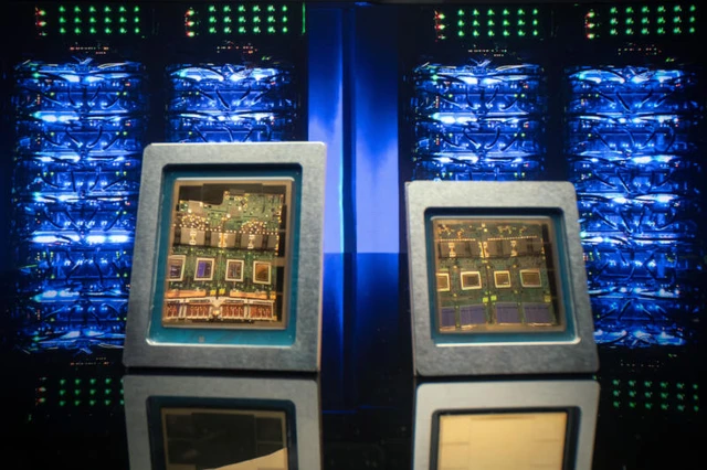
The technological leap for the ninth-generation TPU centers on the transition to a chiplet architecture—an industry-wide trend driven by the physical limitations of lithography and the imperative to increase wafer yields. Each new accelerator is expected to utilize four compute dies. However, this strategy introduces significant engineering hurdles in packaging and interconnects. When multiple large dies are integrated onto a single substrate, the requirements for precision and data transfer speeds between them increase exponentially.
Manufacturing capacity remains the primary bottleneck. It is evident that TSMC, despite its colossal resources, may be unable to handle such volumes alone. This compels Google to consider partnering with Intel. However, a critical technical friction point emerges: packaging technologies differ fundamentally across vendors. Intel's solutions, such as EMIB or EMIB-T, lack direct compatibility with TSMC's CoWoS-L standard, turning the diversification of production into a complex exercise in adapting chip design for different foundries.
The development of proprietary TPUs has spanned a decade, during which the role of these devices has fundamentally evolved. While they were initially designed to optimize specific workloads—such as TensorFlow model training—TPUs have now become the cornerstone of Google's global cloud strategy. Achieving its 2028 targets would transform the company into the world's largest consumer of AI accelerators by volume.
This does not imply a total abandonment of Nvidia procurement, but it radically shifts the balance of power. By maintaining a fleet of millions of proprietary chips, Google gains unprecedented control over infrastructure TCO (Total Cost of Ownership) and supply chain stability. While direct benchmarks comparing the TPU v9 against future Nvidia Rubin and Rubin Ultra lineups are not yet available, one thing is clear: the battle for AI supremacy is shifting from the realm of theoretical teraflops to the domain of industrial scaling and logistical resilience.
 Anthropic’s Strategic Financial Surge Ahead of Its IPO