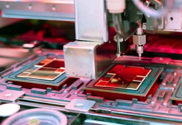
The era of generative AI has fundamentally reshaped the landscape of the semiconductor industry. Traditional two-year hardware refresh cycles have become a prohibitive luxury, giving way to annual and even semi-annual iterations. Google is now pivoting toward an accelerated roadmap for its Tensor Processing Units (TPUs) in a bid to aggressively close the performance gap. This strategy transforms hardware development into a perpetual cycle of innovation, where the velocity of deployment has become a critical factor for survival.
For years, the microelectronics industry operated on a predictable cadence: a new generation of processors arrived every two years, providing the market ample time to adapt and engineers the opportunity to meticulously refine the product. However, the explosive rise of neural networks has completely upended this timeline. Today, even an annual update cycle feels sluggish. Recognizing this, Google is pivoting to an aggressive strategy: Tensor Processing Units (TPUs) will now be updated twice a year.
This acceleration is driven not merely by a desire for dominance, but by stark market imperatives. In an era where the competition for computational power has reached a fever pitch, any delay in silicon iteration translates directly into a loss of momentum in model training. Google’s AI infrastructure leadership has openly acknowledged that even a six-month cycle may prove insufficient, and the company is prepared to further accelerate the development of its custom silicon.
Yet, engineering the perfect chip is only half the battle. The true challenge lies in the realm of logistics and manufacturing. To sustain such a relentless pace, production lines must operate at peak capacity, and testing systems must function flawlessly. The primary "bottleneck" has become the supply chain. Issues can arise from anywhere: a shortage of high-bandwidth memory (HBM) and printed circuit boards (PCBs) to a lack of power components or liquid cooling systems. In this environment, the nature of these challenges shifts hourly; a critical bottleneck identified in the morning can be replaced by a new systemic failure by lunchtime.
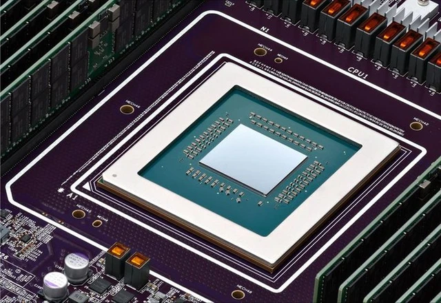
The technical trajectory of the TPU is shifting toward hyper-specialization. In the current generation, Google has bifurcated the workload: the TPU 8t is optimized for heavy-duty model training, while the TPU 8i is dedicated to inference—the stage where queries are executed. The key factor here is not so much the raw power of a single core, but the efficiency of interconnects within the cluster. The integration of ultra-high-speed network channels allows Google to aggregate up to one million TPUs into a single computational system, effectively transforming the company's infrastructure into one of the most powerful supercomputers in history.
The scale of Alphabet's capital expenditure in this endeavor is staggering, with up to $205 billion potentially allocated to infrastructure development this year. Despite this, Google is maintaining a pragmatic strategy. While developing its own TPUs—which the company intends to offer to external clients—it continues to procure Nvidia accelerators, creating a hybrid ecosystem where different chip architectures complement one another.
The geography of TPU production represents a sophisticated symbiosis of American design and Asian execution. Taiwan remains the primary technological epicenter, where MediaTek assists with development and TSMC handles the actual wafer fabrication. Broadcom and Marvell are also integral to the process. However, the final assembly of TPU-based server systems remains concentrated in the hands of American firms, specifically Celestica and Flex.
Looking ahead, Google plans to further deepen its footprint in Taiwan, increasing regional investments by 60%. Furthermore, the company is exploring partnerships with Intel and Samsung for contract manufacturing, packaging, and testing. Such a move would diversify risk and ensure the operational throughput necessary to realize its ambitious plan for accelerated hardware iteration.
 The Horizon of China's Technological Sovereignty in Lithography