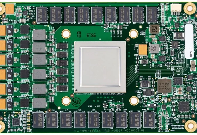
The global shortage of compute capacity has emerged as the primary bottleneck hindering the comprehensive automation of society and the advancement of artificial intelligence. In response to this crisis, Tesla and SpaceX are spearheading the development of TeraFab, a massive semiconductor fabrication facility based in Texas. The initiative is designed to secure the technological sovereignty of Elon Musk’s broader ecosystem by vertically integrating silicon production with its end-use application. It represents a strategic pivot toward an autonomous future—one where robotics and neural networks serve as the fundamental infrastructure of society.
Grimes County, Texas, is becoming the epicenter of one of the most ambitious engineering feats of the decade. Tesla and SpaceX are pooling their resources to construct TeraFab—a specialized fabrication plant dedicated to advanced semiconductors. While initial investments are estimated at $16.8 billion, long-term projections suggest capital expenditures could scale up to $119 billion. The sheer scale of the facility is staggering: with production areas exceeding 9.3 million square meters, it is poised to become one of the largest industrial complexes on the planet.
The strategic imperative behind TeraFab is to bridge the critical chasm between current global chip capacity and the exponential surge in demand for compute resources. In today’s technological arms race, access to cutting-edge process nodes has become a matter of survival; establishing an internal production hub allows the companies to minimize reliance on external vendors and fragile global supply chains.
TeraFab serves as the bedrock for a broader vision of a future dominated by autonomous systems. This includes millions of Optimus humanoid robots, Cybercab autonomous vehicles, and orbital data centers designed to act as processing nodes for global AI training. To power such an ecosystem, chips must be purpose-built for edge computing and inference, enabling data to be processed locally on the device to eliminate the latency inherent in cloud communication.
A cornerstone of TeraFab is the concept of deep vertical integration. The facility will consolidate the production, packaging, and testing of both logic devices and memory modules within a single ecosystem. This architecture enables a recursive optimization loop: real-world performance data from deployed chips can be fed instantly back into the design and manufacturing stages, radically accelerating the iteration cycle for new processor generations.
Intel is also slated to play a role in the project, with its deep expertise in lithography and semiconductor fabrication serving as a potential catalyst for the plant's operational launch. Despite the magnitude of the announcement, financial transparency remains selective; recent public filings from the involved companies rarely detail TeraFab, underscoring the strategic opacity surrounding the development.
Ultimately, TeraFab is more than just an industrial site—it is an attempt to create a closed-loop ecosystem where hardware is engineered specifically for the requirements of software and robotics. By doing so, chip production is transformed from a third-party service into a core strategic asset that will dictate the pace of artificial intelligence evolution.
 The Price of Acceleration: CXMT’s Rapid Push into Memory