The global race for semiconductor supremacy has traditionally centered on lithography and the relentless pursuit of smaller nanometer nodes. Yet, the ability to fabricate a die is only half the battle; final assembly and advanced packaging are what truly dictate the real-world performance of modern systems. While the United States pours billions into reshoring manufacturing, a critical void in packaging expertise is creating a precarious dependency on a single dominant player. This strategic oversight renders the ambition of technological sovereignty a fragile facade, leaving a dangerous disconnect between the physical fabrication of chips and their ultimate realization.
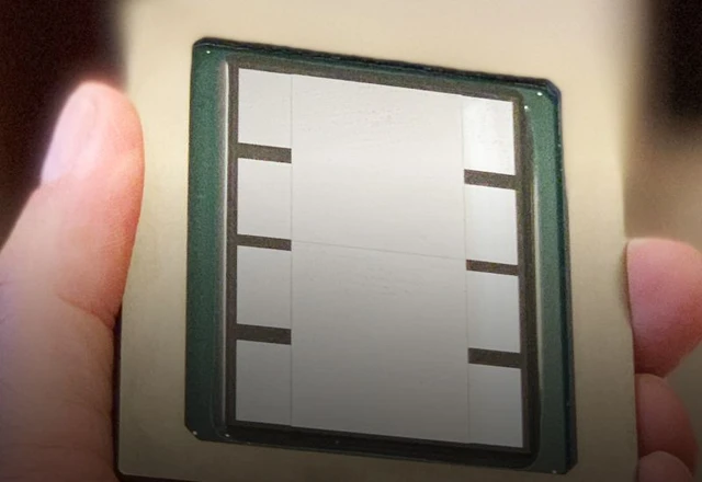
The microelectronics industry is currently navigating a fundamental paradigm shift. While progress was once measured primarily by transistor density per die, the spotlight has shifted toward the concept of heterogeneous integration. Advanced Packaging—the process of combining multiple specialized chiplets onto a single substrate—enables the creation of ultra-powerful systems that would be impossible to implement within a single monolithic chip. It is precisely here that the primary vulnerability of the American tech sector lies.
While Washington remains preoccupied with the "onshoring" of lithography fabs, the critical issue of back-end assembly has remained in the shadows. This strategic oversight has manifested in the political arena: an ambitious plan to establish a specialized research center in Arizona, for which the Biden administration intended to allocate $1.1 billion, has effectively collapsed. The withdrawal of subsidies during Donald Trump's second presidency led to the dissolution of the non-profit organization tasked with leading these developments. Consequently, the U.S. finds itself in a precarious position where investments in chip fabrication are not supported by the necessary packaging infrastructure.
Industry experts emphasize that packaging technologies are second in importance only to the fabrication processes themselves. However, the supply chains in this segment are even more fragile. Currently, the U.S. share of the global packaging services market does not exceed 3%, leaving the industry almost entirely dependent on the Taiwanese giant TSMC.
The surge in artificial intelligence has only intensified the urgency of this problem. For the production of the cutting-edge accelerators procured by Nvidia and other market leaders, CoWoS (Chip on Wafer on Substrate) technology is critical. This method allows computing cores to be integrated with High Bandwidth Memory (HBM) with ultra-low latency. The crux of the issue is that TSMC will be unable to deploy corresponding capacities on U.S. soil until 2028 or 2029.
This creates an illogical logistical loop: chips manufactured at new plants in Arizona must be shipped to Taiwan for packaging and testing, only to be sent back to the U.S. This dependency is further exacerbated by a capacity shortfall; TSMC's CoWoS capabilities lag behind market demand by approximately 30%. The high cost of these services—ranging from $40 to $500 per unit depending on complexity—is forcing some developers to seek alternatives to avoid excessive end-product price hikes and integration risks.
In an attempt to bridge this gap, the private sector is taking the initiative. Intel and Applied Materials are expanding their domestic packaging and equipment manufacturing capacities. A significant milestone is Amkor Technology's plan to invest at least $7 billion in the construction of the first advanced packaging facility in the U.S. This project has already attracted the attention of Apple and Nvidia and will provide critical support for TSMC over the next decade.
Nevertheless, piecemeal investments by individual companies are no substitute for a systemic state strategy. As the market fills with startups offering lower-cost assembly methods and industry consortia emerge, the American industry must realize one thing: true technological sovereignty is impossible without control over the entire product lifecycle—from the first photolithographic layer to the final encapsulation.
 The Evolution of the Apple Home Ecosystem