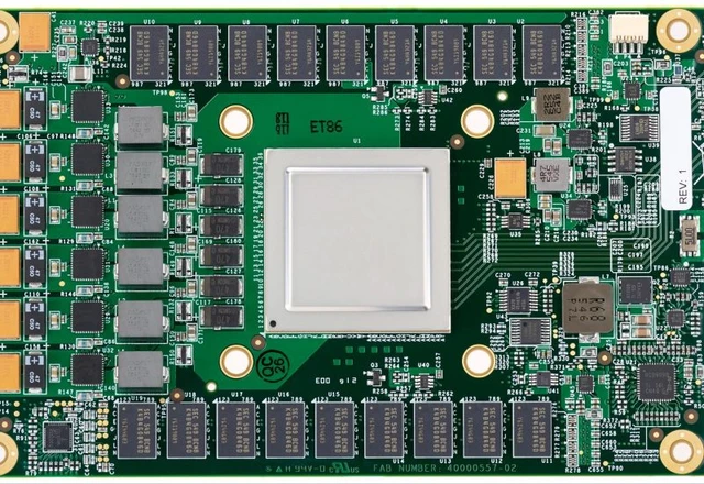
The global race for technological sovereignty has shifted from a mere arms race over hardware acquisition to a contest of engineering prowess and executional precision. In an era of stringent sanctions, the capacity to design complex integrated circuits that are "right-first-time" for mass production has become a critical determinant of survival. Against this backdrop, Chinese engineers are demonstrating surprising efficacy, challenging established Western design paradigms. This qualitative leap is precisely what enables them to circumvent constraints on accessing cutting-edge lithography equipment.
In the semiconductor industry, there is a concept known as "first-pass success"—the ability to design a chip that functions flawlessly after the initial production cycle, eliminating the need for costly and time-consuming respins. For most global firms, this remains an elusive ideal; on modern process nodes, any error in die layout can result in millions of dollars in losses and months of delays. However, insights from within Huawei Technologies reveal that Chinese engineering has developed a unique approach to mitigating these risks.
The shift from Western design methodologies to Eastern ones has exposed a profound gap in how specialist potential is assessed. While the prevailing narrative long favored the superiority of Western schools in system design, practice has proven otherwise: HiSilicon is capable of delivering dozens of complex digital projects annually that move straight to mass production without corrective iterations. This speaks not merely to discipline, but to an elite level of engineering expertise across every stage of the product lifecycle.
Today, this internal capability serves as the bedrock for a strategy of total import substitution. The primary focus is the development of advanced Ascend family accelerators, intended to secure China's autonomy in artificial intelligence. With access to cutting-edge lithography—such as ASML’s EUV systems—restricted, the emphasis has shifted from the physical shrinking of transistors toward the intelligent optimization of the chip's internal architecture.
Of particular interest is the implementation of the LogicHolding approach. This methodology enables increases in processor performance and energy efficiency even when utilizing less advanced manufacturing equipment. Essentially, it is a matter of compensating for lithographic deficits through architectural superiority and a denser, more sophisticated arrangement of logic blocks. The first smartphone chip developed under this principle is expected to serve as tangible proof that engineering ingenuity can overcome the physical limitations of hardware.
Consequently, China's technological leap is fueled not only by state investment but by a fundamental overhaul of its development culture. Moving away from "blind arrogance" toward an acknowledgment of local competencies has fostered a system where design precision becomes the primary weapon against external constraints.
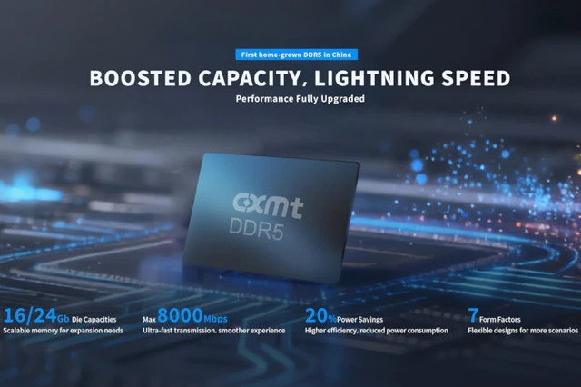 The Price of Acceleration: CXMT’s Rapid Push into Memory