The global race for nanometer supremacy is entering a phase of extreme optimization, where marginal gains in efficiency now dictate leadership across the semiconductor landscape. In a bid to reclaim its status as a technological hegemon, Intel is pivoting heavily toward the expansion of its foundry services. The introduction of the modified 18A-P process node represents a pivotal milestone in this ambitious strategic pivot. Intel is no longer focusing solely on its internal requirements; it is now courting the world's biggest chip designers, who demand a flawless equilibrium between raw performance and power efficiency.
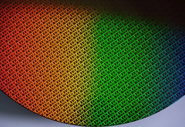
At the VLSI Symposium in Honolulu, Intel officially confirmed the commencement of pilot production for chips based on its 18A-P technology. This development is a highly refined iteration of the existing 18A process, specifically engineered to address one of the most persistent challenges in modern silicon: striking the optimal balance between clock speeds and thermal output. In an industry where every milliwatt is contested, 18A-P represents Intel's strategic effort to create a product appealing to external clients who are traditionally risk-averse when switching suppliers.
The technical specifications of this new iteration are impressively pragmatic. According to Intel's internal benchmarks, the transition to 18A-P enables either a 9% increase in overall system performance or—more critically for the mobile and data center segments—an 18% reduction in power consumption compared to the base 18A process. The thermal profile is particularly noteworthy, with crystal heat characteristics improving by at least 20%. In an era where extreme transistor density inevitably leads to "hot spots," such thermal optimization becomes a decisive factor in the architecture of high-performance systems.
Intel's strategic calculus extends far beyond mere metrics. The company is aggressively scaling its foundry services, aiming to position itself as a viable, full-scale alternative to TSMC. In this context, 18A-P could serve as the catalyst that opens doors for giants like Apple. For Apple, diversifying supply chains is an existential imperative; the current reliance on a single Taiwanese behemoth introduces significant geopolitical and logistical vulnerabilities.
Furthermore, Intel is leveraging its expertise in advanced packaging. As TSMC encounters certain scaling limitations in its packaging services, Intel can offer clients a comprehensive "turnkey" solution, integrating a cutting-edge fabrication process with innovative chiplet packaging and interconnect methods.
From a development standpoint, the migration to 18A-P is designed to be seamless. The design toolset is fully compatible with the base 18A process, meaning there is no need for costly, time-consuming engineer retraining or a complete overhaul of the chip's floorplan. This significantly lowers the barrier to entry for third-party firms, allowing them to migrate to the new process with minimal lead time.
However, the critical question remains: yield. In the semiconductor business, the yield rate is the ultimate arbiter of economic viability. Until Intel demonstrates consistently high yields in mass production, the industry's largest customers will likely remain cautious. Nevertheless, the launch of 18A-P pilot production signals that the company is moving beyond conceptual roadmaps and into the practical execution of its new business model.
 The Speed Limits of Modern Gaming Displays