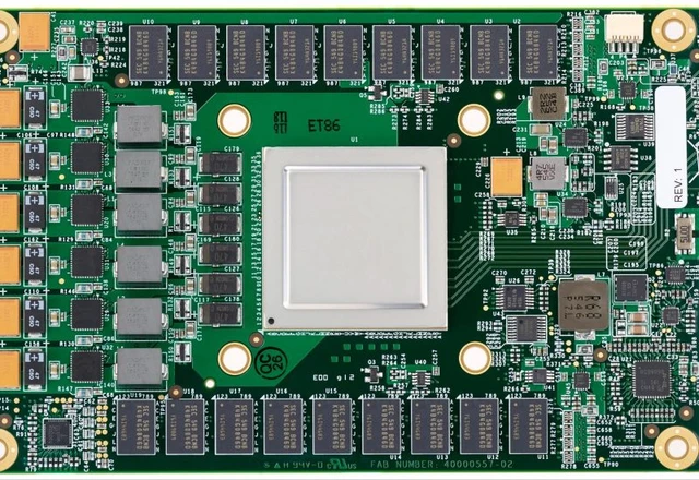
The nanometer race has reached a critical inflection point where simply shrinking transistor dimensions is no longer sufficient to achieve a qualitative leap in performance. TSMC is now pushing beyond the two-nanometer barrier with the unveiling of its A16 process, marking a fundamental paradigm shift in semiconductor manufacturing. This transition is not merely about increasing component density, but about a radical overhaul of how power is delivered to the die. The industry stands on the threshold of an era where energy efficiency has become the primary driver behind the evolution of computing systems.
The current era of microelectronics is defined by a fundamental shift from nanometer-scale precision to angstrom-scale dimensions. Within this context, TSMC is preparing for the mass production of components utilizing the A16 process, which effectively aligns with the 1.6nm node. With the validation phase already complete, the company intends to launch production in the coming quarter, complementing its existing 2nm fabrication lines.
The cornerstone of the A16 technological breakthrough is the implementation of Super Power Rail (SPR)—a backside power delivery system. In traditional architectures, power and signal lines are routed on the same side of the silicon wafer, inevitably leading to crosstalk and limiting layout density. By decoupling these circuits, TSMC can radically reduce electromagnetic interference, enhance clock speeds, and optimize power consumption. Crucially, TSMC has managed to maintain conventional design rules, which is vital for shortening development cycles and accelerating time-to-market for new silicon.
A comparative analysis of A16 against its predecessor, the N2P process, reveals impressive gains. The new technology delivers a performance uplift of 8–10% while maintaining the same power envelope. Alternatively, when operating at current clock speeds, power consumption drops by 15–20%. Simultaneously, transistor density has increased by nearly 10%, enabling the creation of more compact and powerful dies.
These improvements are particularly critical for the artificial intelligence sector. Modern AI accelerators used for training neural networks demand massive amounts of energy and frequently struggle with thermal throttling. Moving power lines to the backside of the die allows for more efficient heat dissipation and more uniform power delivery—a decisive factor when scaling massive AI processors.
The A16 architectural stack extends beyond power routing. It continues the evolution of Gate-All-Around (GAA) transistors, which first debuted in the N2 series. Unlike traditional FinFETs, GAA structures provide superior control over leakage current and significantly increase switching efficiency. Consequently, A16 represents a synergy of two critical vectors: the refinement of transistor geometry and the modernization of the power delivery network.
Despite its technical significance, TSMC views A16 as a pivotal transitional milestone. The company's primary strategic focus remains the A14 process, slated for launch in 2028. It is within A14 that TSMC expects the full culmination of its advancements in backside power delivery and angstrom-scale lithography.
Against this backdrop, the competitive landscape remains fragmented. Samsung Electronics does not plan to implement its SF1.4 process until 2029 at the earliest, focusing currently on stabilizing wafer yields for the SF2 series. Intel, meanwhile, has already introduced its 18A node to the market, yet the transition to mass production for 14A is also not expected until 2028. This underscores TSMC's current leadership in mastering advanced lithographic norms and its ability to set the cadence for the entire semiconductor industry.
 The Price of Acceleration: CXMT’s Rapid Push into Memory