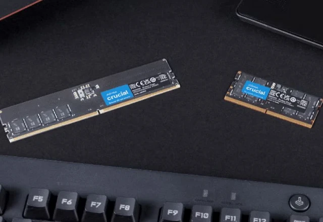
The global semiconductor memory market is undergoing a fundamental transformation, one where agility and the speed of adaptation are superseding mere scaling. The traditional paradigm of expansion—driven by the construction of new fabrication plants—is giving way to a strategy centered on deep optimization and technological modernization. Samsung Electronics is pivoting toward intensive growth, prioritizing the improvement of wafer yields and the migration to cutting-edge process nodes. This strategic shift enables the company to scale supply volumes while minimizing capital expenditure on physical infrastructure.
The memory manufacturing industry is entering a pivotal era where scaling physical footprints is no longer the primary lever for market dominance. Samsung Electronics is recalibrating its priorities, shifting from extensive expansion toward a strategy of maximum efficiency. Rather than commissioning new fabrication plants, the company is betting on improving product yields and accelerating the migration to more advanced process nodes.
At the heart of this strategy is the transition of DRAM production from the 1b node to the more sophisticated 1c process. This modernization allows for increased data density and energy efficiency without requiring additional cleanroom square footage. However, this transition is complicated by the surging demand for HBM4 memory, which demands significant resources and attention, inevitably throttling overall growth rates. According to Omdia analytics, DRAM output is projected to grow by approximately 6% this year, reaching 8.2 million wafers, while growth is expected to decelerate to 1.3% next year, plateauing at 8.28 million wafers.
This internal restructuring of production capacity is leading to a redistribution of workloads across sites. The Pyeongtaek plant is emerging as the primary engine of expansion; through equipment upgrades, its share of total DRAM production is expected to rise from 49.5% to 55.4% by next year. This underscores the company's drive to extract maximum value from its existing assets.
Simultaneously, a different dynamic is unfolding at the Hwaseong complex. Over the last three years, this site has seen stagnation or even negative growth. Here, Samsung is employing a method of "technological recycling": legacy lines that previously produced 2D NAND are being repurposed for DRAM testing and packaging. Given that mature versions of DRAM and NAND accounted for roughly 30% of revenue in 2024, the modernization of these lines unlocks hidden potential for optimization without the need for capital-intensive new construction.
However, such a cautious strategy introduces certain risks in the face of competitor activity. SK hynix is pursuing a far more aggressive trajectory, planning to increase its wafer processing volume by nearly 10% to 6.66 million units. This divergence in approach is gradually narrowing the market gap: while Samsung previously led its competitor in DRAM output by 27%, this advantage could shrink to 13.6% by next year.
In an environment of acute memory shortages, SK hynix’s agility in saturating the market appears more advantageous in the short term. Nevertheless, Samsung’s bet on quality and the technological perfection of its process nodes may yield a superior long-term dividend, transforming operational efficiency into its primary competitive advantage.
 The Dawn of the 2nm Era in the New iMac