The global semiconductor landscape is undergoing a fundamental transformation, one where the dominance of a single player has evolved into the industry's primary systemic risk. Against this backdrop, Intel is embarking on one of the most ambitious pivots in the history of Big Tech: evolving into a full-scale foundry services provider. The sheer scale of recent financial maneuvers suggests that the market is beginning to buy into the viability of this strategy. This is not merely a matter of bolstering the balance sheet; it is about laying the groundwork to challenge TSMC and Samsung at the level of physical fabrication.
Intel's recent financial maneuvers reveal an unexpected trajectory: initial plans to raise $15 billion in capital have evolved rapidly. The final sum has reached $20 billion, and with stock buyback options within a thirty-day window, total investment could climb to $23 billion. For GF Securities analysts, this surge is a critical indicator: Intel isn't merely plugging budget holes; it is aggressively scaling its ambitions within the contract manufacturing segment.
The primary beneficiary of this capital influx will be Intel Foundry Services (IFS). The funds are earmarked for deep modernization and the expansion of production capacities—a critical step in transitioning from a "design-for-self" model to a "produce-for-all" paradigm. A particularly strong signal was sent by CEO Lip-Bu Tan, who personally committed to purchasing company shares. In the world of corporate finance, such a move is interpreted as the ultimate vote of confidence from top management in the chosen strategic direction.
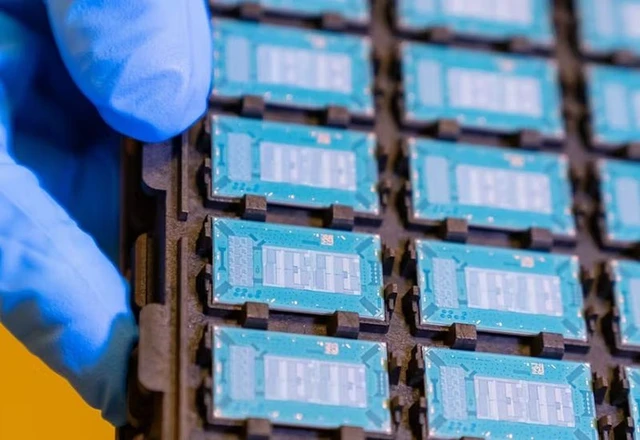
The technological bedrock of this push is the Intel 18A process node. Market expectations suggest that yields and quality at this node have reached a level capable of attracting the most demanding clients, including Apple. However, the true growth potential lies not just in transistor density, but in packaging methodologies. EMIB (Embedded Multi-die Interconnect Bridge) technology, which enables the efficient integration of multiple dies into a single system, is becoming a pivotal selling point for cloud giants.
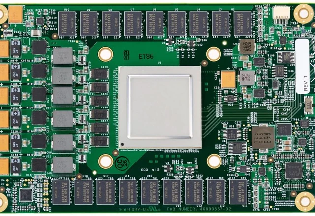
Google and Amazon (AWS), in their quest to develop proprietary custom accelerators for data centers, require the advanced chip packaging that Intel can provide. The economic impact of EMIB adoption is expected to grow exponentially: experts project that revenue from these services will climb from $1.1 billion in 2027 to a staggering $7 billion by 2028.
The road to financial health for the contract business will be long and capital-intensive. The IFS division is expected to reach its break-even point by the fourth quarter of 2027. It is only by 2028 that these operations will begin to exert a noticeable positive influence on the corporation's overall profit margins. Consequently, Intel is playing a long game, transforming its fabrication plants from internal assets into a global service capable of shifting the power dynamics of the semiconductor industry.
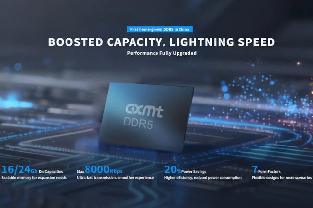 The Price of Acceleration: CXMT’s Rapid Push into Memory