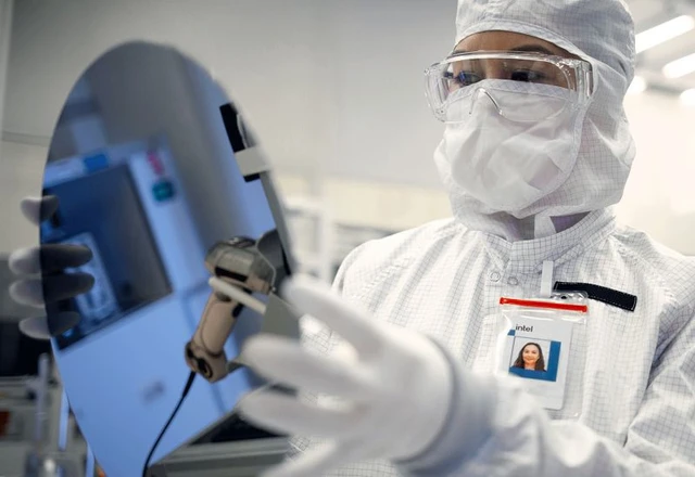
In the semiconductor industry, the success of a new process node is dictated less by theoretical potential than by the cold, hard mathematics of wafer yield. Every migration to a more advanced node is fraught with initial yield instability—a period of high defect rates that can prove fatal to a product's commercial viability. Intel is currently navigating this critical phase with its 14A process, aiming to cement its dominance in chip manufacturing by the end of the decade. Current metrics suggest that the company is resolving these manufacturing hurdles far more rapidly than industry benchmarks would typically dictate.
In the realm of semiconductor manufacturing, "yield"—the percentage of functional dies harvested from a single silicon wafer—is the ultimate metric of success. Traditionally, the early stages of any new lithography process are plagued by low yields, as microscopic defects render a significant portion of the output useless, resulting in staggering financial losses. However, Intel is demonstrating unexpectedly optimistic momentum with its promising 14A process node.
According to data from Morgan Stanley analysts, Intel has managed to push its yield to 50% even before the official launch of pilot production. For the initial phase of node maturation, this represents a major victory, substantially mitigating the risks associated with scaling.
Intel's strategic roadmap positions the 14A process as the successor to the 18A family. Engineering samples based on this new technology are expected by 2028, with full-scale mass production slated for no earlier than 2029. If current trends hold, experts predict that the defect rate could plummet to 10–20% by the first quarter of next year. Such a milestone would allow the company to transition from experimental wafers to the creation of fully realized prototypes for commercial products.
The relationship between die size and the failure rate is non-linear: the larger the chip's surface area, the higher the probability that a critical defect will compromise it. To illustrate this dependency, consider a hypothetical scenario involving Panther Lake processor cores. If these were manufactured using the 14A process with a die area of approximately 114 mm², the increased transistor density would result in a yield of roughly 56.45%.
Conversely, the test chips Intel uses for process calibration are significantly larger, which naturally suppresses their yield to around 40%. However, once the target defect rate of 10–20% is achieved for dies of approximately 100 mm², the proportion of functional chips per wafer could soar to 80–90%. It is important to note that even among "functional" dies, some will fail the rigorous binning process for clock speeds and power efficiency; consequently, the final commercial yield will be slightly lower than the theoretical maximum.
A technological leap of this magnitude is impossible without a corresponding software ecosystem. Currently, the Electronic Design Automation (EDA) tools tailored for 14A are at version 0.5. An update to version 0.9 is expected by this autumn, which will serve as a critical signal to Intel Foundry's external customers that the platform is ready to accept their designs.
The foundation of the 14A rollout is the implementation of ASML’s High-Numerical Aperture (High-NA) EUV equipment. Intel has already integrated the cutting-edge Twinscan EXE:5200B system into its production lines. High-NA lithography enables significantly higher resolution when printing structures, which reduces the number of required exposures and minimizes overlay errors—the very factors driving the observed surge in wafer yield.
 The Speed Limits of Modern Gaming Displays