The global semiconductor market is undergoing a fundamental paradigm shift, pivoting from an era of total globalization toward one of regional resilience. Washington's drive to reshore high-tech manufacturing demands the creation of a comprehensive, end-to-end ecosystem—spanning everything from silicon wafer fabrication to final assembly and testing. Leveraging its dominance in the AI landscape, Nvidia has emerged as a pivotal catalyst in this transition. Strategic investments in advanced chip packaging are effectively transforming Arizona into the new epicenter of global microelectronics.
The modern semiconductor manufacturing stack is bifurcated into two critical stages: wafer fabrication (front-end) and subsequent packaging and testing (back-end). In 2024, a pivotal milestone in this chain was the launch of TSMC's first Arizona facility, specializing in 4nm process nodes. However, access to cutting-edge lithography alone is insufficient for achieving true technological sovereignty. For a chip to become a finished device, it must undergo complex packaging and verification processes—capabilities that have long been the exclusive domain of Asian production hubs.
To bridge this gap, Nvidia has entered into a massive agreement with Amkor, one of the world's leading providers of chip testing and packaging services. The company will provide $1.5 billion in advance payments to expand Amkor's specialized capacity within Arizona. This deal is more than just financial; it is deeply strategic, allowing Nvidia to mitigate logistical risks and accelerate time-to-market by establishing a comprehensive domestic manufacturing cluster. The market reacted instantaneously, reflected in a 15% surge in Amkor's share price.
It is crucial to understand that packaging modern AI accelerators is not merely a matter of mechanical assembly, but a sophisticated engineering feat. We are talking about Advanced Packaging techniques—such as 2.5D and 3D integration—which enable the fusion of the compute die with high-bandwidth memory (HBM). This specific stage currently represents the primary bottleneck for the entire industry.
Nvidia is not alone in its drive toward localization. TSMC also plans to construct two of its own packaging and testing plants in Arizona. The current logistical framework is profoundly inefficient: semi-finished products are shipped from the US to Taiwan for final assembly, only to be shipped back to America. Establishing local capacity will completely eliminate this cross-border cycle.
Under this partnership, Nvidia and Amkor intend to co-develop new packaging technologies, effectively creating a joint R&D center dedicated to increasing on-chip component density. Furthermore, the ecosystem is expanding: Amkor's client base includes AMD, making the infrastructure development in Arizona mutually beneficial for all major players in the US AI hardware market. Thus, a powerful industrial symbiosis is forming—one where government ambitions for reshoring intersect with the pragmatic interests of tech giants.
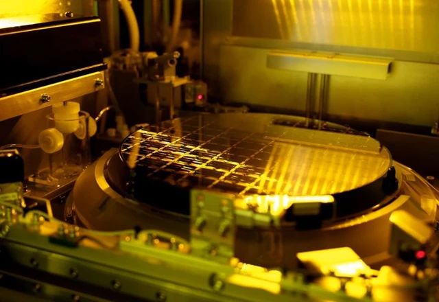
 The Triumph of 3nm Chip Manufacturing